

Beam current affects signal to noise, charging, and resolving power. Find out how and why.
Optimizing Beam Current - SEM
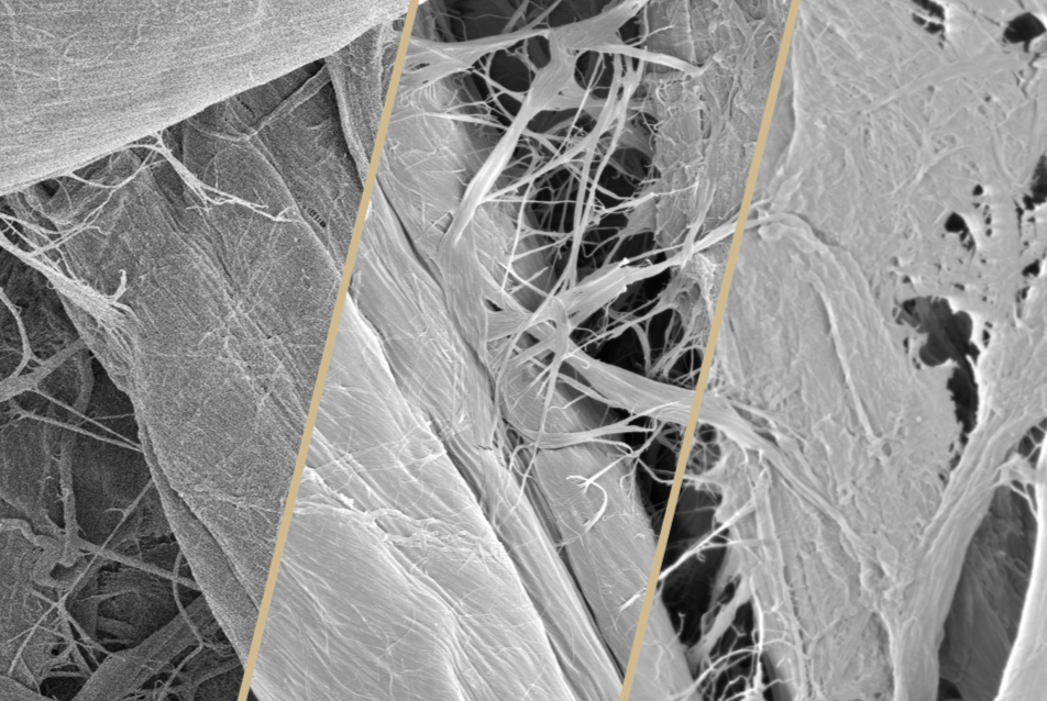
What is beam current? Beam current is a measurement of the number of electrons in the electron beam. In an SEM, beam current has three major impacts on your image: signal to noise (S/N), charging, and resolving power. No two samples are the same, so no single beam current is good for all samples! Below is a guideline to help you optimize beam current for your sample.
Low Signal to Noise (S/N)
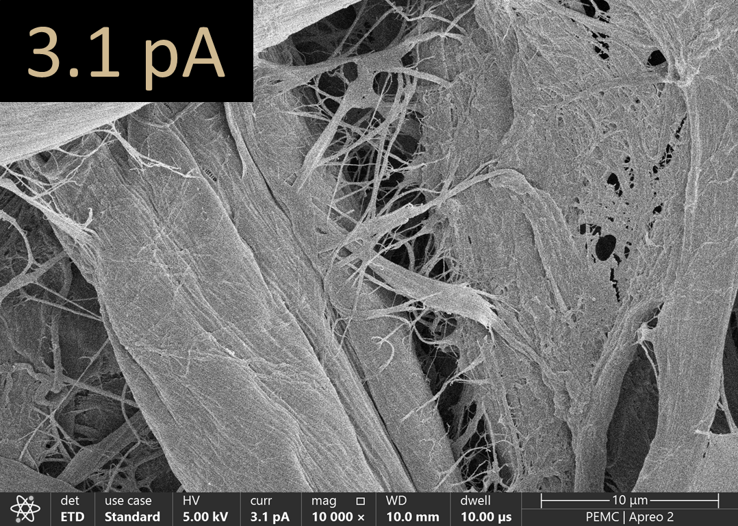
- Signal is low because there are not many electrons hitting the sample.
- Compensate for low S/N by using longer pixel dwell times during image collection.
- There are not many electrons hitting the sample, which reduces charging.
- Allows you to resolve smaller features because the size of the beam is smaller.
High Signal to Noise (S/N)
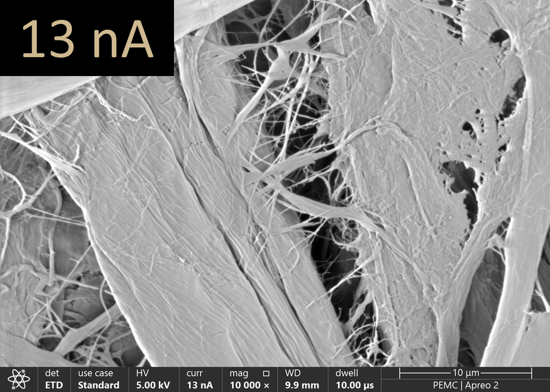
- Many electrons hit the sample, producing a large amount of signal.
- The amount of noise does not change, so the S/N ratio improves.
- There are a large number of electrons hitting the sample surface, which take longer to be grounded, especially by a non-conductive material.
- Resolution decreases when the size of the beam becomes larger than the features of interest.
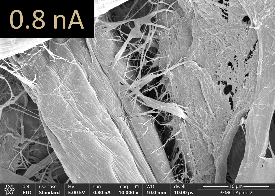
Sufficient Signal to Noise (S/N)
- An optimal beam current produces sufficient S/N to produce quality images.
- While optimizing beam current, also experiment with pixel dwell times. Dwell time has a large impact on S/N too.
- An optimal beam current produces little to no charging.
- Coating samples with a conductive material can help reduce charging too.
- An optimal beam current allows you to resolve features of interest.
- Resolving smaller features requires the use of a lower beam current.
Low Signal to Noise (S/N)
- Signal is low because there are not many electrons hitting the sample.
- Compensate for low S/N by using longer pixel dwell times during image collection.
- There are not many electrons hitting the sample, which reduces charging.
- Allows you to resolve smaller features because the size of the beam is smaller.
High Signal to Noise (S/N)
- Many electrons hit the sample, producing a large amount of signal.
- The amount of noise does not change, so the S/N ratio improves.
- There are a large number of electrons hitting the sample surface, which take longer to be grounded, especially by a non-conductive material.
- Resolution decreases when the size of the beam becomes larger than the features of interest.
Sufficient Signal to Noise (S/N)
- An optimal beam current produces sufficient S/N to produce quality images.
- While optimizing beam current, also experiment with pixel dwell times. Dwell time has a large impact on S/N too.
- An optimal beam current produces little to no charging.
- Coating samples with a conductive material can help reduce charging too.
- An optimal beam current allows you to resolve features of interest.
- Resolving smaller features requires the use of a lower beam current.
Click the button to the right to keep on learning!
On to Pixel Dwell Time!Click the button to the right to keep on learning!
On to Pixel Dwell Time!