

EQUIPMENT
This page provides descriptions of the equipment in the PEMC and summarizes their capabilities. If you are looking for example write-ups for publications, take a look at our Example Write-Ups page.
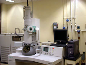
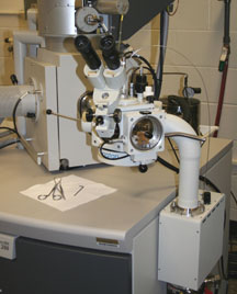
Transmission Electron Microscopes
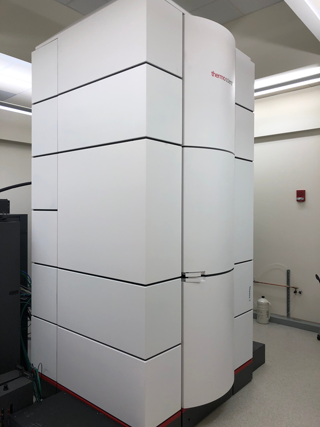
Our double aberration-corrected Themis-Z TEM is equipped with a high-coherence and high-brightness Schottky field emission electron gun (X-FEG), and an electron gun monochromator to provide a super high spatial resolution of 65pm at 300 kV and an energy resolution of 100 meV. Atomic resolution imaging is also available at 60 kV and 80 kV for beam-sensitive materials with imaging and probe correctors. Segmented STEM detectors enable differential phase contrast related imaging such as STEM-iDPC. The system contains a high-speed, high-throughput, quad-silicon drift detectors (Super-X) optimized for rapid x-ray collection and when combined with STEM enables EDS spectral mapping down to the atomic scale. This system is also equipped with Gatan Digiscan™ to produce spectral maps from electron energy loss spectroscopy (EELS) data in a high speed. A dual-EELS spectrometer permits the user to collect low-loss and core-loss EELS simultaneously to produce, rapidly and routinely, atomic resolution EELS spectrum images. With a dedicated tomography holder, 3D reconstruction is capable on the nano scale for both imaging and chemical analysis.
Major Features of this high-resolution instrument are:
imaging:
- 60 - 300 kV monochromated Schottky field emission electron gun.
- Probe and image aberration corrected.
- Atomic resolution in both TEM and STEM with resolution of <65 pm at 300 kV.
- Scanning TEM (STEM).
- Single tilt and double tilt holder available.
Energy Dispersive X-ray (EDX) Spectroscopy
- EDX spectroscopy (also known as EDS) allows elemental composition analysis of elements at or above atomic number 5.
- Quad-silicon drift detector (Super-X).
- EDX spectral mapping down to the atomic scale.
Electron Energy Loss Spectroscopy (EELS)
- EELS provides bonding and oxidation state information.
- Gatan Quantum 965 Detector.
Integrated differential Phase contrast (IDpc)
- IDPC allows light element detection in STEM.
Electron Tomography
- 3D reconstruction via tilt series image collection.
- 3D imaging and 3D elemental composition.
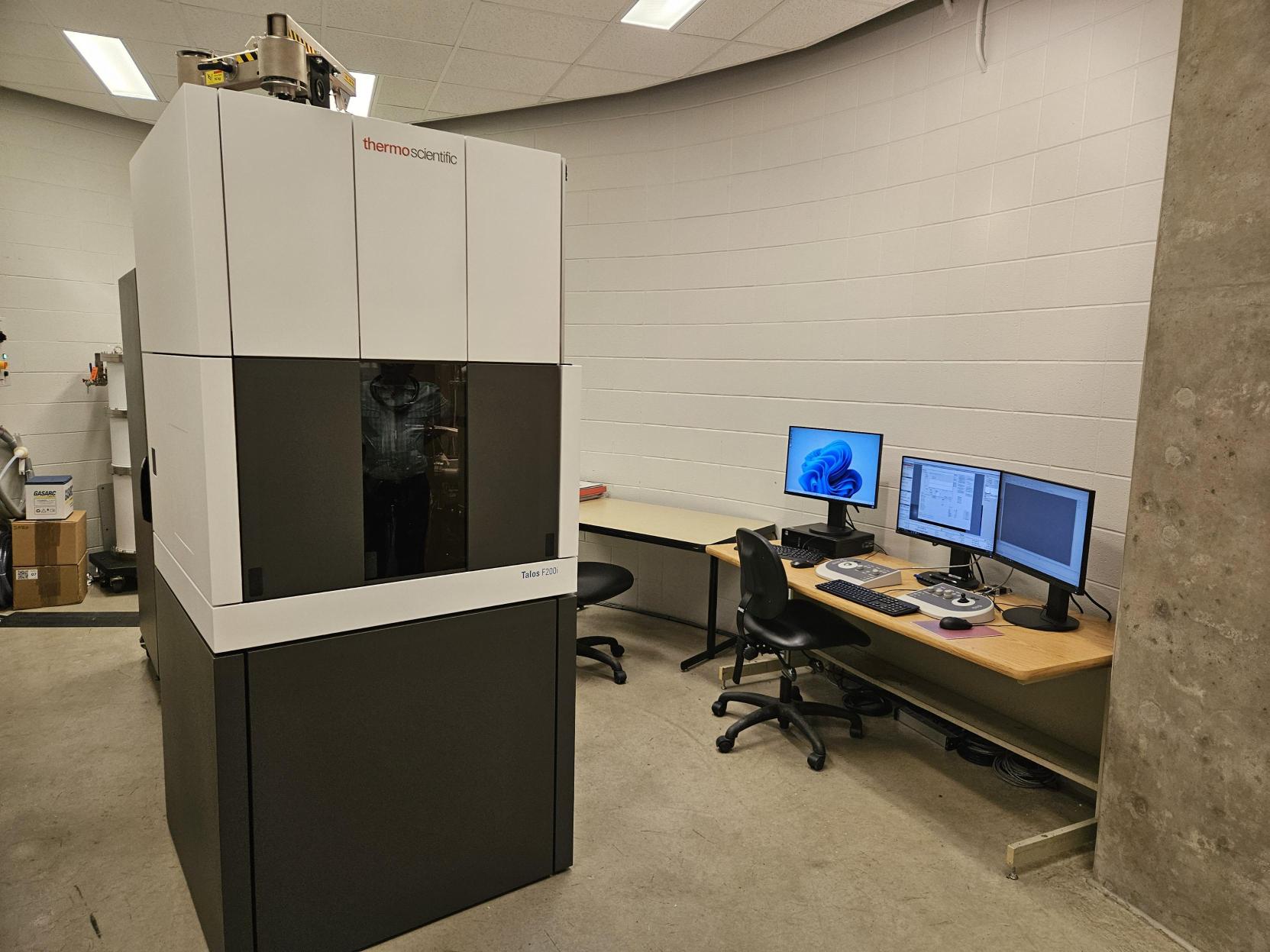
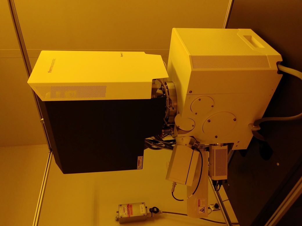
Talos F200i ttransmission electron microscope operated at 200 kV (also available at 80kV) is capable of TEM and STEM modes. It is equipped with speed enhanced Ceta camera (CMOS) for TEM and new Panther STEM detectors (STEM BF, LAADF and HAADF), as well as Super-X EDS with four silicon drift detectors for large collection solid angle. The user friendly TEM and STEM auto alignment makes the microscope operation comparatively easy. The new "Click tilt" function (SmartCam) allows users to orient the sample to a zone axis more easily.
Major Features of this high-resolution instrument are:
imaging:
- 200 kV field emission electron gun.
- On-axis Panther bright-field/dark-field (BF/DF) detector.
- Line resolution of ≤ 0.1 nm in TEM.
- Scanning TEM (STEM) with resolution of 0.16 nm.
- Single tilt and double tilt holder available.
Energy Dispersive X-ray (EDX) Spectroscopy
- EDX spectroscopy (also known as EDS) allows elemental composition analysis of elements at or above atomic number 5.
- Quad-silicon drift detector (Super-X).
- EDX spectral mapping available.
differential Phase contrast (Dpc)
- DPC allows light element detection in STEM.
Major Features include:
imaging:
- 200 KV LaB6 filament electron gun.
- Bottom mount Gatan US1000 2Kx2K.
- Single tilt holder and low background double tilt holder available.
Energy Dispersive X-ray (EDX) Spectroscopy
- EDX spectroscopy (also known as EDS) allows elemental composition analysis of elements at or above atomic number 5.
- Oxford Instruments X-MAX SDD EDX detector
- Point analysis.
Electron Tomography
- 3D reconstruction via tilt series image collection.
Major Features include:
imaging:
- 120 kV tungsten filament electron gun (typically operated at 80 kV for high contrast in biological samples).
- Side-mount wide-angle CCD camera.
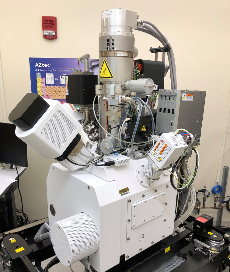
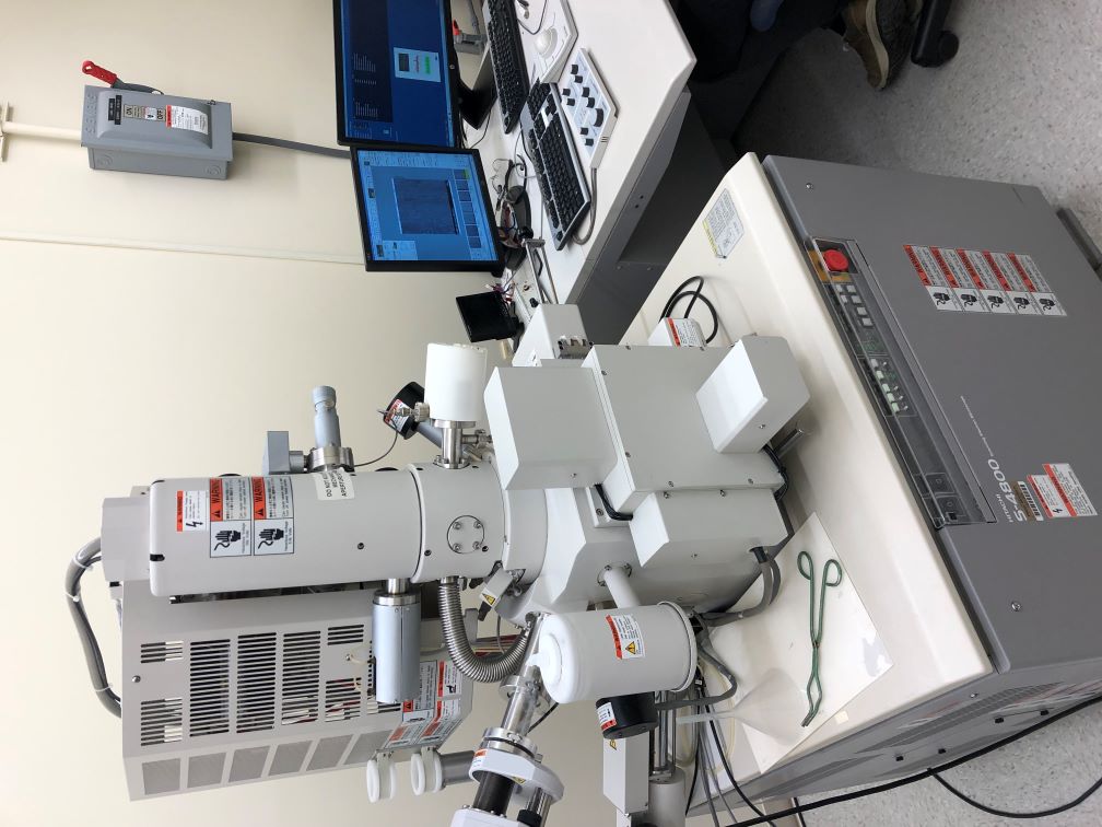
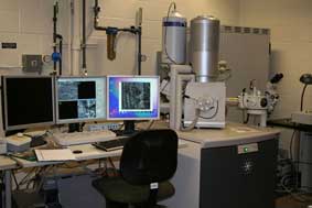
Scanning Electron Microscopes
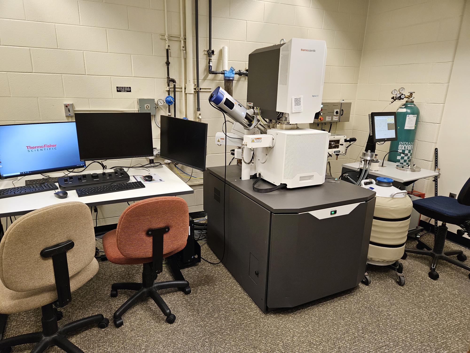
Major Features of this high-resolution instrument are:
imaging:
- Three modes of high vacuum operation allow high resolution imaging of a wide range of conductive or coated materials.
- Low vacuum detectors allow imaging of uncoated non-conductive samples.
- Multiple detectors are available to allow imaging with contrast based on surface topography or average atomic number.
- Automated image stitching enables collection of large area maps at high resolution.
Electron Channelling Contrast Imaging (ECCI) and Electron Channelling Pattern (ECP):
- ECCI allows image collection with crystallographic contrast to observe crystalline grains and detect dislocations.
- ECP employs a rocking electron beam to produce Kikuchi patterns.
Cryo-SEM
- Loading frozen samples and keeping them frozen throughout imaging allows SEM images to be acquired of hydrated samples, aqueous suspensions, and materials containing volatiles.
- Imaging at low temperatures can reduce sample damage for beam-sensitive materials and reduce heat-related sample movement.
Energy Dispersive X-ray (EDX) Spectroscopy
- EDX spectroscopy (also known as EDS) allows elemental composition analysis of elements above atomic number 5.
- Single point analysis or area mapping is available.
Major Features of this high-resolution instrument are:
imaging:
- Two modes of high vacuum operation allow high resolution imaging of a wide range of conductive or coated materials.
- Multiple detectors are available to allow imaging with contrast based on surface topography or average atomic number.
- Automated image stitching enables collection of large area maps at high resolution.
Focused Ion Beam (FIB):
- Gallium FIB for site specific milling, machining, deposition, and lamella prep.
Electron backscatter Diffraction (EBSD):
- Analysis of crystalline material to analyze grain size and orientation.
Energy Dispersive X-ray (EDX) Spectroscopy:
- EDX spectroscopy (also known as EDS) allows elemental composition analysis of elements above atomic number 5.
- Single point analysis or area mapping is available.
Scanning Transmission EM (STEM):
- STEM allows analysis of very thin samples.
Major Features of this high-resolution instrument are:
imaging:
- Two modes of high vacuum operation allow high resolution imaging of a wide range of conductive or coated materials.
- Low vacuum detectors allow imaging of uncoated non-conductive samples.
- Multiple detectors are available to allow imaging with contrast based on surface topography or average atomic number.
- Automated image stitching enables collection of large area maps at high resolution.
serial block face imaging:
- Serial sectioning is performed using an in-situ ultramicrotome.
Scanning Transmission EM (STEM):
- STEM allows analysis of very thin samples.
Major Features of this instrument are:
imaging:
- High vacuum operation allows imaging of a wide range of conductive or coated materials.
- Low vacuum detectors allow imaging of uncoated non-conductive samples.
- Multiple detectors are available to allow imaging with contrast based on surface topography or average atomic number.
Energy Dispersive X-ray (EDX) Spectroscopy
- EDX spectroscopy (also known as EDS) allows elemental composition analysis of elements above atomic number 5.
- Single point analysis or area mapping is available.
Focused Ion Beam (FIB)
- Gallium FIB for site specific milling, machining, deposition, and lamella prep.
Full Environmental SEM (ESEM)
- ESEM allows controlled changes in humidity up to 100% RH with simultaneous SEM imaging.
Major Features of this instrument are:
imaging:
- High vacuum operation allows imaging of a wide range of conductive or coated materials.
- Low vacuum detectors allow imaging of uncoated non-conductive samples.
- Multiple detectors are available to allow imaging with contrast based on surface topography or average atomic number.
Energy Dispersive X-ray (EDX) Spectroscopy:
- EDX spectroscopy (also known as EDS) allows elemental composition analysis of elements above atomic number 5.
- Single point analysis or area mapping is available.
Electron backscatter Diffraction (EBSD):
- Analysis of crystalline material to analyze grain size and orientation.
Major Features of this high-resolution instrument are:
imaging:
- Two modes of high vacuum operation allow high resolution imaging of a wide range of conductive or coated materials.
- Multiple detectors are available to allow imaging with contrast based on surface topography or average atomic number.
- Automated image stitching enables collection of large area maps at high resolution.
Major Features of this instrument are:
imaging:
- Cold cathode field emission gun (cFEG) produces high brightness, low energy spread, and a small source size.
- High vacuum operation allows imaging of a wide range of conductive or coated materials.
- Multiple detectors are available to allow imaging with contrast based on surface topography or average atomic number.
Energy Dispersive X-ray (EDX) Spectroscopy:
- EDX spectroscopy (also known as EDS) allows elemental composition analysis of elements above atomic number 5.
- Single point analysis or area mapping is available.
Support Equipment
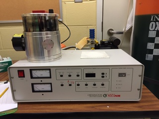
Cressington 208HR turbo-pumped sputter coater
Used primarily for platinum deposition, but iridium deposition is available on request.
The SPI-Module line of modular sputter coaters and carbon coaters are optimized for Au/Pd coating and Carbon coating for all SEM and EDS applications.
- Au/Pd sputter to disperse charge on SEM samples.
- SPI Vacuum Control Base is equipped with both a diode magnetron sputtering head and carbon coater.
- Sputtering is achieved with Ar+ plasma and Au/Pd (60:40) target for SEM sample coating.
- Carbon coater head uses carbon fiber filaments (provided).
- Work chamber accommodates up to 6 pin-mount specimen stubs (12.5mm dia).
Typically used for EBSD sample preparation to produce a highly polished surface.
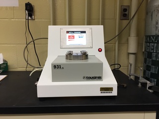
Tousimis 931 CPD
Used for controlled dehydration of materials (typically biological samples) in preparation for SEM imaging.
The MultiPrep™ System is a programmable machine that enables precise semiautomatic sample preparation of a wide range of materials for microscopic (optical, SEM, FIB, TEM, AFM, etc.) evaluation.
Capabilities include parallel polishing, angle polishing, site-specific polishing or any combination thereof. It provides reproducible results by eliminating inconsistencies between users, regardless of their skill. Dual micrometers (pitch and roll) allow precise sample tilt adjustments relative to the abrasive plane. A rigid Z-indexing spindle maintains the predefined geometric orientation throughout the grinding/polishing process. Digital indicators enable quantifiable material removal, which can be monitored real-time, or preset for unattended operation. Variable speed rotation and oscillation maximize use of the entire grinding/polishing disc and minimize artifacts. Adjustable load control expands its capability to handle a range of small/delicate to large samples.
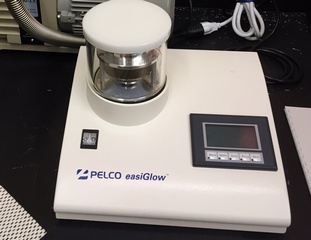
Glow discharge can be used to make TEM grids or glass coverslips hydrophilic prior to applying an aqueous sample. This is frequently used to improve sample dispersion during negative staining TEM prep or to disperse aqueous suspensions across coverslips prior to drying for SEM imaging.
The NanoMill system is fully automated and easily programmable. Adjustable ion beam energies, milling angles, specimen rotation, and cryogenic specimen cooling parameters afford maximum flexibility to ensure the optimal preparation of a wide variety of specimens. The ion beam can be targeted to a specific area of interest. A secondary electron detector is used to image the ion-induced secondary electrons that are generated from the targeted area of the specimen.
- Removes amorphous and implanted layers.
- Ultra-low energy ion source, variable from 50 eV to 2 keV.
- Concentrated argon ion beam, with a diameter down to 1 µm at 2 keV.
- Milling angle range: -10° to +30°.
- Liquid nitrogen-cooled specimen stage.
- Ion-induced secondary electron imaging of the specimen.
- Oil-free vacuum system with a base pressure of 3 x 10⁻⁵ Pa and operating pressure of 1 x 10⁻² Pa.
The PIPS II system incorporates the patented WhisperLok® with the X, Y positioning stage for precise centering of the milling target. The PIPS II system incorporates a 10-inch touch screen for ease of use and increased control and reproducibility of the milling process.
The Digital Zoom Microscope monitors the polishing process in real-time and the color images can be stored in Gatan’s DigitalMicrograph® software for review and analysis while the sample is in the TEM.
- Improved collimated beam provides useable voltages as low as 100 volts for rapid and damage-free preparation of FIB lamella
- Low energy focusing Penning Ion Guns - Improved low energy milling FIB prepared samples.
- Variable energy from 100 V to 8.0 kV - Improved low energy milling for reduction in amorphous layer for correct TEMs.
- LN2 specimen cooling - Eliminates artifacts 10-inch color touch screen control - Simple but full control from the graphical user interface (GUI).
- Digital Zoom Microscope - Operates in real-time while milling.
- Color image storage in DigitalMicrograph - Ability to store and use optical images with the TEM EELS data in the same format.
- Pelco Oven for Microwave fixation
- Pelco easiSlicer Vibratome
- Reichert Ultracut E ultramicrotomes
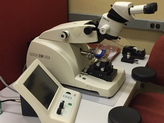 Leica UC6 Ultramicrotome
Retired Equipment
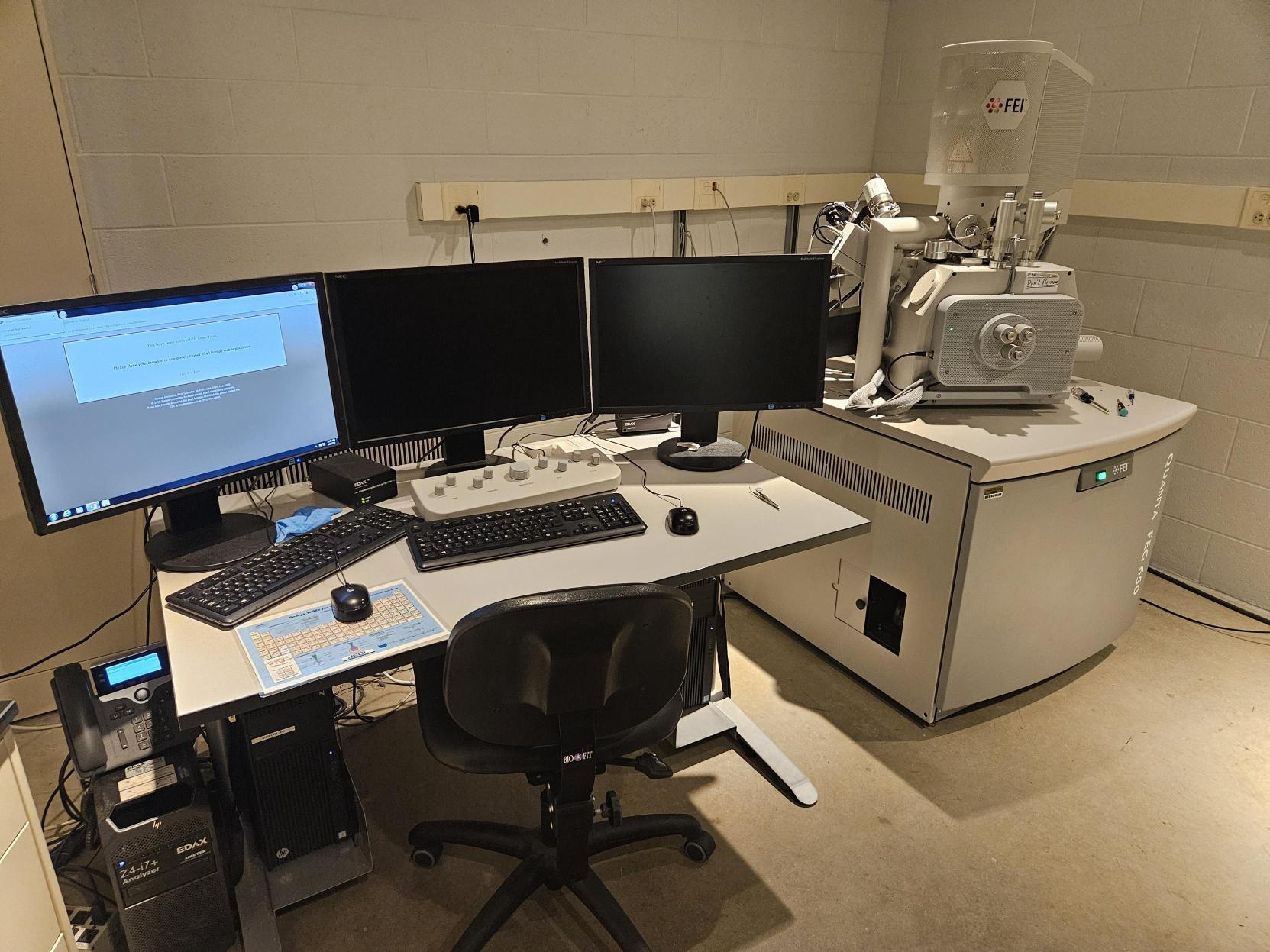
Major Features of this high-resolution instrument are:
High vacuum imaging:
- Everhart Thornley detector (ETD): routine imaging
- Through-the-Lens detector (TLD): high magnification/resolution
Low vacuum imaging:
- Low vacuum detector (LVD)-lower magnifications
- Helix detector (Helix)-high magnification/resolution
Back-scattering imaging using the Gaseous Analytical Detector (GAD):
- High vacuum and low vacuum
STEM detector:
For very thin samples and high vacuum only Cryo imaging utilizing the GATAN Alto 2500 cryo system Elemental Analysis utilizing Electron Dispersive X-ray analysis (EDX)
- Oxford INCA Energy 250 system with 30mm window
The CM-100 is a basic TEM and has a magnification range from 20x to 510,000 and accelerating voltage from 40 to 100kV.
Special Features:
Low-dose for automatic shift to new area after focusing or focusing on same are but with low beam intensity to minimize beam damage prior to recording.
Specimen relocation system. Gatan Orius side mount CCD camera
- 30mm window
 The cryo systems on the NOVA nanoSEM and the Quanta 3D FEG microscopes are optimized for use on field-emission microscopes. They consist of a freezing unit, a turbo-pumped cryo preparation unit, and a cryo stage that attaches to the microscope stage. The cryo system permits flash freezing of samples in liquid nitrogen slush followed by high vacuum sublimation of unbound water, Pt coating to minimize charge build-up and imaging at temperatures down to ~160C.
Please send any questions/comments/concerns regarding the content on this page to snbienz@purdue.edu.