Optimizing SEM Parameters
The information on this page is designed to provide guidance for optimization of beam current, beam voltage, and dwell time in SEM. No two samples are alike, so try to understand the impact of each parameter in the context of your sample and the information you are hoping to learn from the SEM images that you collect.
Contents
Each link below will scroll down the page to take you directly to your parameter of interest.
Optimizing Beam Current
What is beam current? Beam current is a measurement of the number of electrons in the electron beam. Beam current has three major impacts on your image: signal to noise (S/N), charging, and resolving power. No two samples are the same, so no single beam current is good for all samples! Below is a guideline to help you optimize beam current for your sample.
Low Signal to Noise (S/N)
- Signal is low because there are not many electrons hitting the sample.
- Compensate for low S/N by using longer pixel dwell times during image collection.
- There are not many electrons hitting the sample, which reduces charging.
- Allows you to resolve smaller features because the size of the beam is smaller.
High Signal to Noise (S/N)
- Many electrons hit the sample, producing a large amount of signal.
- The amount of noise does not change, so the S/N ratio improves.
- There are a large number of electrons hitting the sample surface, which take longer to be grounded, especially by a non-conductive material.
- Resolution decreases when the size of the beam becomes larger than the features of interest.
Sufficient Signal to Noise (S/N)
- An optimal beam current produces sufficient S/N to produce quality images.
- While optimizing beam current, also experiment with pixel dwell times. Dwell time has a large impact on S/N too.
- An optimal beam current produces little to no charging.
- Coating samples with a conductive material can help reduce charging too.
- An optimal beam current allows you to resolve features of interest.
- Resolving smaller features requires the use of a lower beam current.
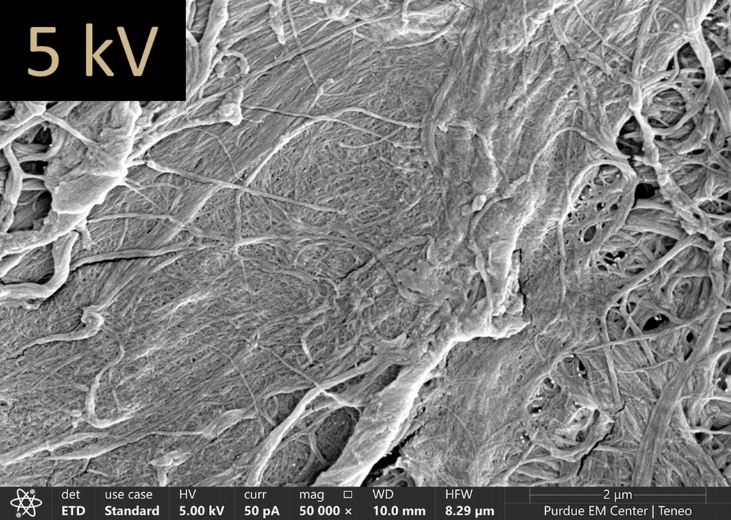
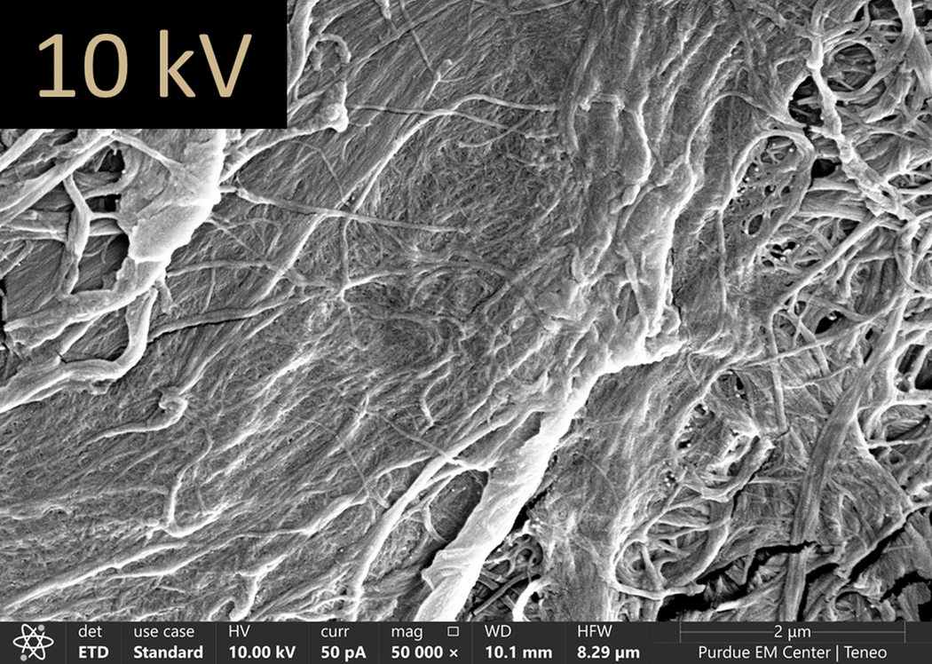
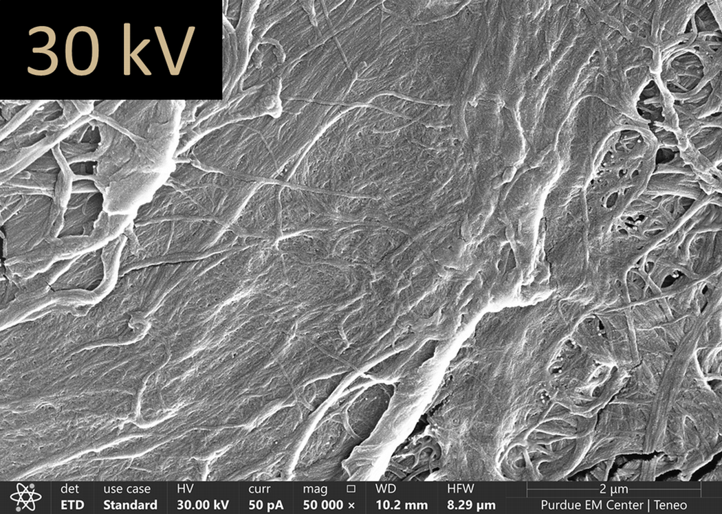
Optimizing Beam Voltage
What is beam voltage? Beam voltage is a measurement of the potential energy of the electrons in the electron beam. Beam voltage has two major impacts on your image: penetration depth (i.e. interaction volume) and signal intensity. No two samples are the same, so no single beam voltage is good for all samples! Below is a guideline to help you optimize beam voltage for your sample.
Shallow Penetration Depth
- Ideal for evaluating the surface of samples.
- Allows resolution of small surface features.
- Shallow penetration depth means that the electron beam interacts with fewer atoms in the sample, producing fewer secondary electrons for SE imaging.
- A lower voltage incident beam leads to lower voltage backscattered electrons which are less likely to be detected in BSE imaging.
Deep Penetration Depth
- Causes fine surface detail to become blurred, or vanish completely.
- Can cause surface edges to look semi-transparent, making the image appear blurry.
- Produces high intensity SE images because the electron beam interacts with a larger volume in the sample to produce a large number of secondary electrons.
- The high voltage of the incident beam leads to high voltage backscattered electrons which are easily detected in BSE imaging.
Minimizes Penetration Depth
- An optimal beam voltage minimizes penetration depth to avoid losing any features of interest.
- An optimal beam voltage produces sufficient intensity without compromising penetration depth.
- If intensity is still too low to produce high quality images, beam current and dwell time can be adjusted to improve signal to noise (S/N).
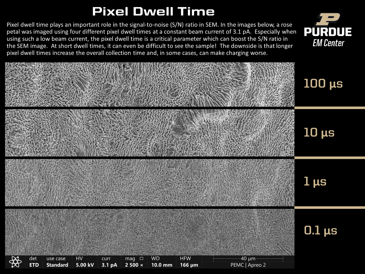
Pixel Dwell Time
Pixel dwell time plays an important role in the signal-to-noise (S/N) ratio in SEM. In the images below, a rose petal was imaged using four different pixel dwell times at a constant beam current of 3.1 pA. Especially when using such a low beam current, the pixel dwell time is a critical parameter which can boost the S/N ratio in the SEM image. At short dwell times, it can even be difficult to see the sample! The downside of longer pixel dwell times is they increase the overall collection time and, in some cases, can make charging worse.